Overview
Within the dynamic semiconductor industry, there is a current trend away from conventional monolithic chip architectures and towards more modular, chiplet-based designs. This shift involves more than just a modification in production methods. It signifies a substantial advancement in the way the electronics sector imagines, creates, and distributes the electronic parts that power the contemporary planet. In the post-Moore's Law age, chiplet-based architectures are becoming a catalyst for innovation and a possible way to sustain the exponential development in computing performance.
Every Internet of Things (IoT) device needs a different set of features, such as memory, computing power, sensor technology, and connection; thus, developing these features using the conventional semiconductor system on a chip (SoC) development cycle is just too costly and time-consuming. As a result, a lot of creative goods are never released. Monolithic chips do have an alternative, though, in the form of silicon chiplets, which can be produced at a very cheap cost and enable the rapid development of tailored functionality using modular building blocks. Despite the unique technological and commercial difficulties that chiplets present, the semiconductor industry is undoubtedly embracing the idea and creating solutions to advance chiplet architectures.
Recently, chiplet-based solutions have become apparent as a promising technology to extend Moore's law across several prominent industry semiconductor vendors and cloud providers, such as Intel, AMD, Broadcom, and Amazon. A variety of factors have contributed to their incredible rise, including avoiding extremely large die size for higher yields, enabling product diversification through mix-and-match techniques for cost savings and reuse, and encouraging heterogeneous integration, which involves integrating chiplets from various process nodes for function, cost, and performance optimization.
Figure 1: Integration of Chipset across the Semiconductor Value Chain
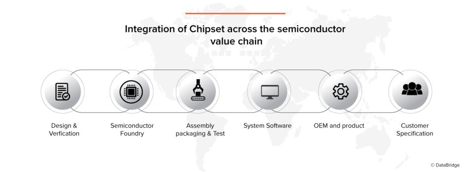
Source: DBMR Analysis
Factors Influencing the Adoption of Chiplet
Challenges Faced during the Chiplet Architecture and Integration
Advantages of Chiplet Technology
Comparing chiplet-based architectures to conventional monolithic System-on-Chips (SoCs), several benefits are apparent. These benefits include improved functionality, lower power consumption, and increased design freedom. Specialized chiplets are predicted by several experts to become a common element in consumer gadgets as cutting-edge technology continue to progress.
Even while conventional chipsets now control the majority of computer technology in electronic devices, it is clear that this trend is about to change in the future. As cutting-edge technology progresses, experts predict that specialized chiplets will become widely used.
Heterogeneous chiplet integration is currently a rapidly expanding market. Both AMD and Intel are producing microprocessors in large quantities that include heterogeneous integrated packaging technology and chiplet designs. The M1 Ultra chip from Apple was unveiled in March 2022. Chiplet architecture is used in this chip, which improves Mac PC performance. We are still in the early phases of chiplet development and manufacturing. But as industry standards solidify, heretofore unthinkable computing models will surface.
Global System-on-Chip (SoC) market has witnessed a substantial growth owing to the increasing demand of SoC in multiple applications including smart devices, autonomous vehicle, portable medical devices and others. Adding to this, rising investment by different government bodies towards setting up manufacturing and production facilities supplements the growth in forecast period. According to Data Bridge Market Research analysis, the market for global System-on-Chip (SoC) market is projected to grow at a compound annual growth rate (CAGR) of 8.55% from 2022- 2029.
To learn more about the study, visit: https://www.databridgemarketresearch.com/reports/global-system-on-chip-soc-market
Several Opportunities and Challenges around the Internet of Things (IoT) Market
Figure 1: Incorporation of Chipset in different IOT devices
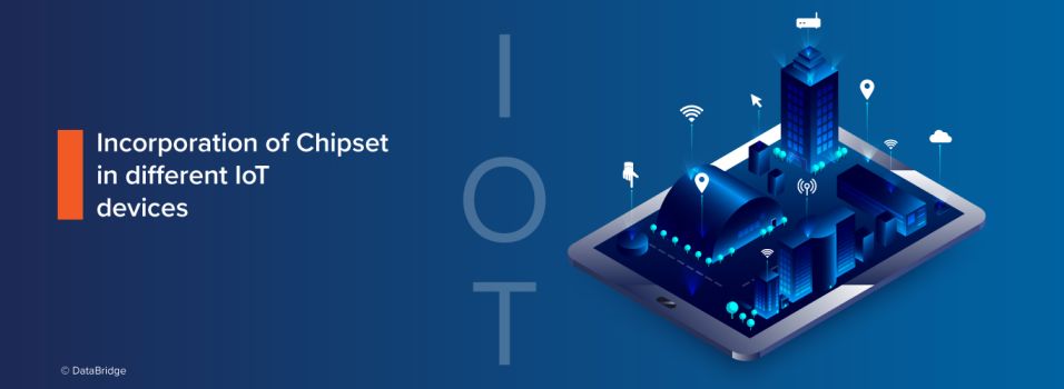
Source: DBMR Analysis
To reach cutting-edge performance, semiconductor investment has been concentrated on device miniaturization; however, this is not the best approach for Internet of Things devices. As part of the worldwide push towards digital transformation, it has been anticipated that the Internet of Things (IoT) will revolutionize enterprises of all sizes with the introduction of 5G and cloud computing. For at least the next few years, it is anticipated that global spending on the Internet of Things will increase at double-digit rates.
IoT has an impact on every facet of society, including corporations, government, and consumers. Industries such as manufacturing, transportation, and utilities are making significant investments in this new technology. Additionally, consumers will drive demand for smart devices that keep them updated about their home and health.
As more and more unique use cases emerge, the growing number of IoT use cases offers great potential for semiconductor manufacturers who supply the underlying silicon-based components as well as OEMs looking to offer cutting-edge solutions. But to make these new use cases possible and advance the market even further, the price of IoT devicesmore especially, the silicon chips that power their intelligence must come down. The goal of semiconductor investment over the past 50 years has been to improve the integrated circuit performance of single monolithic chips used in high-performance applications. As a result, the size of each individual transistor inside semiconductor chips has been continuously decreasing.
Businesses in the semiconductor supply chain have reinvested in IoT nodes that are older and more well-established, but this strategy is unlikely to last. In response to the IoT market, semiconductor manufacturers have made a second wave of investments to employ the same monolithic system on a chip (SoC) technique to reuse previous, established node sizes for use in mixed-signal Internet of Things applications. This is demonstrated by the fact that even with the introduction of newer, smaller process nodes, there is still a significant demand for wafers at bigger node sizes. Semiconductor companies are spending millions of dollars on this massive challenge of migrating analogue functionality from 55 nm and 40 nm to 22 nm. The migration procedure is more difficult and expensive as geometries become smaller.
It has been witnessed that the IoT industry is anticipated to grow significantly for technology companies over the next ten years, Chip manufacturers will aim to build a portfolio of products that will enable them to cater to a wide range of potential uses in diverse sectors. However, given the existing monolithic architecture, which presents issues across numerous dimensions, attaining this at an adequate pricing point will be exceedingly challenging due to the variety of IoT use cases.
Global Internet of Things (IoT) solutions market is witnessing a substantial growth in recent years owing to rapid development of 5g infrastructure for high speed connectivity. Adding to this, rising smart cities initiatives, increasing cloud adoption and utilization of more connected devices supplements the growth of overall IoT market in the forecast period. According to Data Bridge Market Research analysis, the market for global Internet of Things (IoT) solutions market is projected to grow at a compound annual growth rate (CAGR) of 29.30% from 2022- 2029.
To learn more about the study, visit: https://www.databridgemarketresearch.com/reports/global-iot-solutions-market
Chiplets Act as an Aid in Removing the Entry-Barriers for IoT
Monolithic processors are not always the best way to construct mixed-signal Internet of Things devices. Using chiplet architectures is an alternate method that enables the use of several chiplets on a single substrate or in a single package, each with a distinct process node size. Compared to the SoC approach, these kinds of architectures offer a number of advantages to IoT product developers including lesser investment and production costs with lower cost of specialization. Apart from this, other benefits incorporate shorter time to market, lower supply risks for OEMs and simpler architectural partitioning.
OEMs only need to create the specialized chiplets needed for their application and integrate them with commercially available chiplets for the standard functionality, the chiplets strategy also results in lower design costs for any given end product.
Faster prototyping: OEMs and semiconductor companies can mix and match different silicon blocks, including custom chiplets, to create a trial product for quick market testing, instead of needing to invest heavily in developing a new monolithic chip and making sure all the blocks work correctly on the chosen node size
Simpler upgrades: By adding new functionality to a chip without completely redesigning it, functional blocks from a "silicon library" of third-party intellectual property (IP) could be selected, saving testing and validation time.
This is especially helpful if some features are evolving more quickly than others, as is the case with ML chips right now.
By enabling OEMs to source their functional blocks from several suppliers instead of just one, chiplet designs help to lower supply risk.
Adoption of the Chiplets will Present a Gleaming Future in the Future
The increasing variety of possible low-cost Internet of Things applications is driving the chiplet approach's growth. Chiplets adaptability, quick time to market, and lower development and manufacturing costs make it evident that they have the potential to power the next wave of innovative, affordable IoT solutions. With the aid of these designs, original equipment manufacturers (OEMs) can effortlessly integrate cutting-edge digital and analogue features into their final products, offering greater design flexibility in addition to optimal performance. The use of a mix-and-match strategy can also result in lower development costs for these items because the special features can be created as chiplets and subsequently paired with commercially available chiplets. The streamlined process of development and transition to manufacturing also results in a significant improvement in time to market.
Semiconductor businesses can also benefit from this technique. With chiplets, semiconductor businesses will be able to keep their portfolios smaller, cut development costs and timeframes, and offer more optimal products for a wider range of applications. The semiconductor industry's ongoing progress in packaging and interconnects to facilitate these use cases is evidence of this desire. Integration technologies will keep developing to support the full range of IoT devices, from extremely complex ML-enabled autonomous car sensors—where performance is crucial—to more affordable smart tags for consumer use.
Conclusion
Chiplets are a welcome departure from conventional monolithic chip techniques and will open the door to a plethora of innovative, inexpensive Internet of Things devices that were previously unthinkable. Both OEMs and semiconductor businesses can only benefit from this.
Chiplet technology has the potential to completely transform a wide range of industries, such as space exploration, where modular and scalable systems are essential, telecommunications for 5G networks and automotive electronics for advanced driver-assistance systems (ADAS).
With traditional scaling posing challenges to the semiconductor industry, chiplet-based designs are emerging as a potent alternative that could propel the next generation of technological developments. With their unparalleled flexibility, low cost, and capacity to customise functionality to meet individual requirements, chiplets mark a dramatic departure from the traditional approach to electronic design. The skill and desire of designers and engineers in the industry to adopt and develop chiplet technology will be critical in determining the direction of electronics as we approach this new reality.
DBMR has served more than 40% of Fortune 500 firms internationally and has a network of more than 5000 clients. Our Team would be happy to help you with your queries. Visit, https://www.databridgemarketresearch.com/contact
Contact Us