Global Silicon Wafer Reclaim Market
市场规模(十亿美元)
CAGR :
% 
 USD
0.64 Billion
USD
4.58 Billion
2024
2032
USD
0.64 Billion
USD
4.58 Billion
2024
2032
| 2025 –2032 | |
| USD 0.64 Billion | |
| USD 4.58 Billion | |
| % | |
|
全球矽晶圓回收市場細分,按晶圓直徑(300 毫米)、回收方法(機械、化學)、技術工藝(光刻、化學氣相沉積 (CVD)、蝕刻、離子注入、薄膜沉積)、最終用戶行業(半導體製造商、集成設備製造商 (IDM)、離子
全球矽片回收市場規模
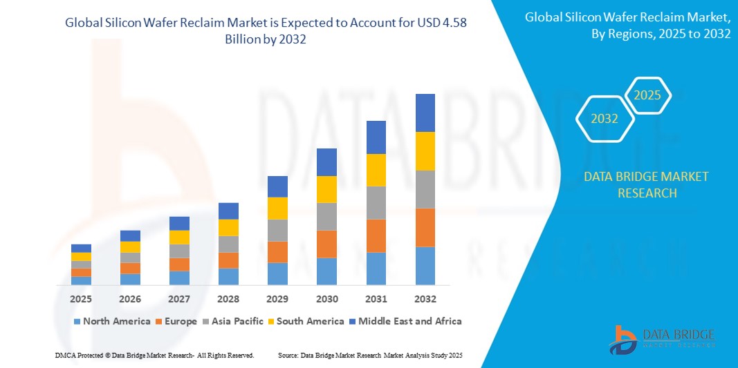
- 2024 年全球矽片回收市場規模為6.4 億美元 ,預計 到 2032 年將達到 45.8 億美元,預測期內 複合年增長率為 32.5%。
- 全球矽片回收市場的成長受到對具有成本效益的半導體製造、可持續發展計劃的需求不斷增長以及太陽能等可再生能源技術的日益普及的推動。
全球矽片回收市場分析
全球矽晶圓回收市場正穩步成長,這得益於電子產業對經濟高效的半導體製造和永續發展計畫日益增長的需求。隨著全球對消費性電子產品、汽車半導體和光伏電池的需求不斷增長,製造商正致力於降低生產成本和減少環境影響。回收矽晶圓是從廢棄晶圓中回收並再加工用於監測和測試的,這提供了一個極具吸引力的解決方案。這使得晶圓廠能夠在不影響製程控制的情況下重複使用材料,從而降低材料成本並減少浪費。
消費性電子、汽車和太陽能等關鍵產業正推動這一成長,因為它們依賴先進的半導體,並順應綠色製造趨勢。此外,5G、物聯網和人工智慧技術的擴張也加劇了對半導體的需求,間接支持了回收市場。晶圓回收也符合全球ESG目標,有助於推動循環經濟策略,並吸引註重負責任資源利用的企業。
晶圓拋光、清洗和檢測技術等回收製程的進步顯著提高了回收晶圓的質量,使其適用於高精度應用。此外,現代晶圓廠對300毫米晶圓的使用日益增多,也為專業的回收服務創造了機會。
然而,市場也面臨挑戰。晶圓回收所需的精度、污染風險以及嚴格的品質控制仍然是重大障礙。此外,並非所有廢舊晶圓都適合回收,需要專門的設備和專業知識來確保穩定的產量,這可能會限制新參與者的進入。
報告範圍與全球矽片回收市場細分
|
屬性 |
全球矽片回收市場洞察 |
|
涵蓋的領域 |
|
|
覆蓋國家 |
北美洲
歐洲
亞太
中東和非洲
南美洲
|
|
主要市場參與者 |
|
|
市場機會 |
|
|
加值資料資訊集 |
除了對市場價值、成長率、細分、地理覆蓋範圍和主要參與者等市場情景的洞察之外,Data Bridge Market Research 策劃的市場報告還包括深入的專家分析、定價分析、品牌份額分析、消費者調查、人口統計分析、供應鏈分析、價值鏈分析、原材料/消耗品概述、供應商選擇標準、PESTLE 分析、波特分析和監管框架。 |
全球矽片回收市場趨勢
“永續性與技術進步重塑晶圓回收實踐”
- 全球矽片回收市場的一個重要且不斷發展的趨勢是,人們越來越重視永續的生產實踐。半導體製造商正在將晶圓回收作為其ESG目標的一部分,以減少浪費和碳足跡,同時優化資源利用率。
- 晶圓拋光、表面處理和粒子檢測的技術進步使得再生晶圓的品質更高,能夠滿足半導體工廠的嚴格標準,從而提高接受度和可用性。
- The growing demand for 300mm and larger wafer sizes in semiconductor production is pushing reclaim service providers to upgrade their facilities with more automated and precision-driven equipment.
- Integration of AI-driven quality inspection and data analytics tools is enabling real-time defect detection, improving process efficiency, and reducing reclaim cycle times.
- With the rise of IoT, 5G, and AI-driven devices, the demand for cost-effective testing wafers has surged—driving the use of reclaimed wafers in monitoring and test processes, especially for advanced node fabrication.
Global Silicon Wafer Reclaim Market Dynamics
Driver
“Rising Demand for Cost Efficiency, Circular Economy, and Semiconductor Innovation”
- The rising cost of prime silicon wafers and the increasing focus on sustainable manufacturing are driving semiconductor companies to adopt wafer reclaiming as a cost-effective and environmentally responsible alternative.
- The expansion of the global semiconductor industry, driven by demand for smartphones, EVs, AI, and IoT devices, is increasing the need for reclaimed wafers for equipment monitoring, testing, and process qualification.
- Government regulations and industry-wide sustainability goals are encouraging companies to reduce silicon waste and energy use, boosting the appeal of reclaim and reuse strategies.
- Advancements in reclaim technologies—such as improved wafer stripping, polishing, and inspection—are enabling better quality control and wider application of reclaimed wafers across 150mm, 200mm, and 300mm formats.
- The growth of semiconductor fabs in emerging markets such as Southeast Asia, India, and Eastern Europe is opening new opportunities for regional reclaim service providers and partnerships with foundries and IDMs.
Restraint/Challenge
“High Cost, Technical Complexity, and Limited Adoption in Developing Economies”
- The high capital investment required for reclaiming equipment such as stripping tools, polishing systems, and advanced metrology tools presents a significant entry barrier for small and mid-sized reclaim facilities.
- Technical complexity in achieving defect-free reclaim wafers, especially for advanced nodes, poses challenges in maintaining quality standards for reuse in critical process applications.
- Limited awareness about the economic and environmental benefits of wafer reclaim particularly in developing countries restricts broader market penetration.
- Inconsistent global standards for wafer reclaim processes, and lack of certifications in emerging markets, hinder uniformity in reclaim quality and reduce cross-border demand.
- Handling ultra-thin wafers or wafers with complex materials (e.g., SOI, GaN) introduces reliability risks, demanding highly controlled environments and skilled personnel for effective reclaim.
Global Silicon Wafer Reclaim Market Scope
The market is segmented on the basis of Wafer Diameter, Reclaim Method, Technology Process and
End-User Industry
By Wafer Diameter
The Global Silicon Wafer Reclaim Market, based on wafer diameter, is categorized into less than 200 mm, 200–300 mm, and greater than 300 mm segments. The <200 mm segment caters to older-generation semiconductor applications, including automotive, analog devices, MEMS, and power electronics. These wafers are widely reclaimed due to their cost sensitivity and widespread use in industrial and consumer electronics. Despite lower performance compared to larger wafers, their reclaimability makes them essential in cost-driven sectors. The 200–300 mm segment dominates the market, owing to its broad adoption in mainstream semiconductor manufacturing. Foundries and integrated device manufacturers (IDMs) widely utilize these wafers for producing logic, memory, and power ICs. Reclaiming 200–300 mm wafers offers significant savings and supports sustainability initiatives, making it the most lucrative segment. The >300 mm segment, though still nascent, is poised for long-term growth. These larger wafers are primarily used in advanced, high-density semiconductor fabrication, including for AI, HPC, and data center applications. As the semiconductor industry gradually moves towards 450 mm wafer production, this segment will become more prominent, driven by efficiency and yield advantages. However, reclaim processes for >300 mm wafers are more complex and still under development.
- By Reclaim Method
Based on reclaim method, the Global Silicon Wafer Reclaim Market is segmented into Mechanical and Chemical processes. The Mechanical reclaim method involves physical techniques such as grinding, polishing, and cleaning to remove surface layers and defects from used wafers. This method is cost-effective and widely adopted for wafers with minor damage or limited contamination. It is favored in applications where reclaimed wafers are used for non-critical processes like equipment calibration, monitoring, or as test wafers. The Chemical reclaim method uses chemical etching, stripping, and cleaning processes to remove layers from the wafer surface. This method is more precise and suitable for reclaiming wafers with heavy contamination or intricate circuit patterns. It allows for better surface quality and reuse in more advanced semiconductor processes. Chemical reclaim is gaining traction due to its effectiveness in maintaining wafer integrity and performance, despite being more expensive and complex.
- By Technology Process
The Global Silicon Wafer Reclaim Market, when segmented by technology process, includes Photolithography, Chemical Vapor Deposition (CVD), Etching, Ion Implantation, and Thin-film Deposition. Each of these processes plays a vital role in semiconductor manufacturing and significantly benefits from reclaimed wafers. In photolithography, reclaimed wafers are used to test alignment and pattern accuracy, reducing the need for new, expensive wafers during process trials. CVD processes utilize reclaimed wafers to evaluate film deposition uniformity and thickness without compromising production resources. Similarly, in etching, these wafers are instrumental in developing etch recipes and monitoring etch rates. Ion implantation benefits from reclaimed wafers by using them in beam calibration and dopant profiling, helping improve accuracy while minimizing waste. Lastly, thin-film deposition processes, including sputtering and evaporation, leverage reclaimed wafers to assess film adhesion, consistency, and stress performance. This segmentation highlights the critical role of reclaimed wafers in optimizing production efficiency, reducing costs, and supporting equipment calibration across multiple advanced semiconductor fabrication processes.
- By End-User Industry
The Global Silicon Wafer Reclaim Market, by end-user industry, is segmented into Semiconductor Manufacturers, Integrated Device Manufacturers (IDMs), Consumer Electronics, Automotive Electronics, Solar Energy, and Telecommunications. Semiconductor manufacturers and IDMs represent the largest share due to their continuous demand for cost-effective wafer recycling solutions in process testing, tool calibration, and equipment maintenance. Consumer electronics drive demand through high-volume production of devices such as smartphones, tablets, and laptops, where wafer reclaim helps reduce production costs. The automotive electronics sector is also expanding rapidly, fueled by the growth of electric vehicles (EVs) and advanced driver-assistance systems (ADAS), which rely on precise and affordable semiconductor testing solutions. In the solar energy industry, reclaimed wafers are increasingly used for testing photovoltaic cell production processes and material efficiency. Lastly, the telecommunications segment benefits from reclaimed wafers in the development of high-frequency and 5G-enabled chips, supporting R&D efforts while maintaining budget constraints. This segmentation underscores how a broad range of technology-driven industries are adopting silicon wafer reclaim to enhance sustainability and cost-effectiveness.
Global Silicon Wafer Reclaim Market Regional Analysis
- 北美約佔全球晶圓回收市場的25%,這得益於其成熟的半導體生態系統和對永續性的高度重視。美國在該地區處於領先地位,受成本效益、環境法規以及美國《晶片法案》(CHIPS Act)等舉措的推動,主要晶圓廠(如英特爾、格芯)採用回收晶圓進行設備校準和測試。
- 歐洲佔了約20%的市場份額,主要得益於其強勁的汽車和工業電子產業。德國和英國尤其註重資源優化和綠色製造,利用回收晶圓來降低生產成本,同時遵守嚴格的環保標準。
- 亞太地區佔據主導地位,佔40%至70%的市場。中國、日本、韓國和台灣等主要國家和地區擁有先進的半導體和太陽能電池製造基礎設施。亞太地區憑藉其龐大的晶圓廠、成本敏感的生產模式以及政府支持的舉措,成為再生晶圓成長最快的地區。
- 拉丁美洲是一個新興市場,約佔全球總量的8%,其中巴西和墨西哥是主要成長點。這些市場在電子產品和太陽能板部署方面正在擴張,而回收晶圓則提供了一種經濟實惠且可持續的解決方案。
- 中東和非洲目前約佔全球市場的7-8%。該地區的成長主要得益於太陽能專案的增加和電子產品製造業的擴張。阿聯酋、沙烏地阿拉伯和南非政府正在推廣有利於晶圓回收解決方案的永續發展實踐。
北美矽片回收市場洞察
北美矽晶圓回收市場正穩步成長,這得益於半導體產業對經濟高效且可持續的晶圓再利用需求的不斷增長。由於主要半導體製造商的佈局,以及《晶片法案》(CHIPS Act)等政府推動國內生產和回收的舉措,美國引領了該地區的成長。 300毫米晶圓因其在先進晶片製造領域的廣泛應用而佔據市場主導地位。此外,強有力的監管政策對循環經濟實踐的支持以及環保製造技術的日益普及,進一步推動了北美市場的擴張。
歐洲矽片回收市場洞察
歐洲矽晶圓回收市場正穩步成長,這得益於該地區對永續性、成本效益和技術進步的高度重視。德國、法國和英國等國家憑藉其強大的半導體製造和汽車電子產業,在矽晶圓回收應用方面處於領先地位。對回收和綠色製造實踐的日益重視,正鼓勵半導體晶圓廠採用晶圓回收技術,以減少材料浪費並最大限度地降低環境影響。此外,在歐盟半導體創新基金的支持下,研發活動的增加也推動了回收晶圓在測試、校準和非關鍵生產流程的應用。電信、再生能源和消費性電子等產業之間技術融合的不斷加強,進一步增強了對矽晶圓回收的需求。
亞太矽片回收市場洞察
亞太地區引領矽晶圓回收市場,這得益於中國大陸、台灣、韓國和日本等國家和地區的半導體製造業。晶圓回收高度重視成本效益和高產量,廣泛應用於設備校準、製程驗證和降低原料消耗。 5G、人工智慧、電動車和再生能源技術推動了裝置製造的快速發展,進一步提升了回收晶圓在非關鍵測試和監控方面的應用。此外,政府旨在促進半導體自主權和永續製造的支持措施與回收帶來的循環經濟效益高度契合。隨著該地區晶圓廠規模不斷擴大和多元化發展,大型和中型回收設施都在投資先進的回收技術,以滿足日益增長的需求並提高製程可靠性。
拉丁美洲矽片回收市場洞察
拉丁美洲的矽晶圓回收市場正處於成長初期,這得益於新興電子製造業活動和再生能源領域投資的不斷增加。巴西和墨西哥等國家正開始採用晶圓回收實踐,以降低生產成本並支持當地半導體和太陽能光電產業的永續發展計畫。隨著地區晶圓廠產能的擴大,回收晶圓越來越多地用於設備校準、製程開發和光伏電池生產。儘管由於回收基礎設施和市場認知度有限,回收率仍然不高,但政府在清潔能源和數位化方面的激勵措施正在激發人們的興趣。展望未來,晶圓廠營運商、研究機構和政策制定者之間的協調努力對於擴大回收規模並將循環經濟實踐融入該地區的半導體生態系統至關重要。
中東和非洲矽片回收市場洞察
中東和非洲的矽晶圓回收市場正在興起,主要由太陽能光電製造、電子組裝和研究設施的早期投資所驅動。阿聯酋、南非和沙烏地阿拉伯等國家正逐步探索晶圓回收技術,以支持永續發展目標並減少新興半導體相關業務中的浪費。在這些設施中,回收晶圓越來越多地用於設備校準和測試,為新晶圓提供了經濟高效的替代方案。然而,技術專業知識有限、回收基礎設施缺乏以及該地區政策支援差異等挑戰阻礙了該技術的快速應用。隨著各國政府推動工業化和循環經濟計劃,晶圓廠營運商、清潔技術供應商和學術機構之間的合作對於擴大回收能力並在中東和非洲地區半導體供應鏈中建立永續的實踐至關重要。
全球矽片回收市場份額
全球矽片回收業主要由知名公司主導,包括:
- 純晶圓
- RS科技公司
- 奈米矽
- 艾德萬泰克
- KST世界公司
- 諾埃爾科技
- 鳳凰矽業
- Optim 晶圓服務
- 矽谷微電子
- 新菱株式會社
全球矽片回收市場的最新發展
- 2024年5月,領先的矽晶圓回收服務供應商NanoSilicon Corp.推出了其下一代回收工藝,該工藝能夠在300毫米晶圓上實現超低顆粒數量。這項創新旨在滿足先進半導體製造日益增長的品質需求,同時提高回收效率並縮短處理時間。
- 2024年3月,RS Technologies Co., Ltd.宣布擴建其位於台灣的回收設施,以滿足亞太地區代工廠和整合設備製造商 (IDM) 日益增長的需求。新生產線專注於採用先進的化學清洗和拋光技術回收200毫米和300毫米晶圓。
- 2024年1月,美國矽片回收公司Pure Wafer與一家領先的太陽能板製造商達成策略聯盟,為非關鍵太陽能應用提供回收矽片。此舉旨在支持太陽能產業降低成本並推動循環經濟。
- 2023 年 11 月,Shinryo Corporation 為其回收服務推出了智慧晶圓可追溯系統,利用 RFID 和區塊鏈技術追蹤晶圓生命週期並確保半導體產業客戶的流程透明度。
- 2023年8月,環球晶圓株式會社在其位於韓國和日本的回收工廠投資了人工智慧驅動的缺陷檢測系統,以提高檢測準確性並優化晶圓回收率。此舉與公司推動晶圓服務數位轉型的策略相契合。
SKU-
Get online access to the report on the World's First Market Intelligence Cloud
- Interactive Data Analysis Dashboard
- Company Analysis Dashboard for high growth potential opportunities
- Research Analyst Access for customization & queries
- Competitor Analysis with Interactive dashboard
- Latest News, Updates & Trend analysis
- Harness the Power of Benchmark Analysis for Comprehensive Competitor Tracking
研究方法
数据收集和基准年分析是使用具有大样本量的数据收集模块完成的。该阶段包括通过各种来源和策略获取市场信息或相关数据。它包括提前检查和规划从过去获得的所有数据。它同样包括检查不同信息源中出现的信息不一致。使用市场统计和连贯模型分析和估计市场数据。此外,市场份额分析和关键趋势分析是市场报告中的主要成功因素。要了解更多信息,请请求分析师致电或下拉您的询问。
DBMR 研究团队使用的关键研究方法是数据三角测量,其中包括数据挖掘、数据变量对市场影响的分析和主要(行业专家)验证。数据模型包括供应商定位网格、市场时间线分析、市场概览和指南、公司定位网格、专利分析、定价分析、公司市场份额分析、测量标准、全球与区域和供应商份额分析。要了解有关研究方法的更多信息,请向我们的行业专家咨询。
可定制
Data Bridge Market Research 是高级形成性研究领域的领导者。我们为向现有和新客户提供符合其目标的数据和分析而感到自豪。报告可定制,包括目标品牌的价格趋势分析、了解其他国家的市场(索取国家列表)、临床试验结果数据、文献综述、翻新市场和产品基础分析。目标竞争对手的市场分析可以从基于技术的分析到市场组合策略进行分析。我们可以按照您所需的格式和数据样式添加您需要的任意数量的竞争对手数据。我们的分析师团队还可以为您提供原始 Excel 文件数据透视表(事实手册)中的数据,或者可以帮助您根据报告中的数据集创建演示文稿。