Abstract
In the rapidly evolving landscape of semiconductor technology, chip packaging plays a pivotal role in enabling the creation of smaller, faster, and more powerful electronic devices. As the demand for increased functionality in devices grows, companies are under constant pressure to offer more components to their clients within limited form factors. This white paper explores the recent advancements in chip packaging, such as 2.5D and 3D packaging, advanced materials, and heterogeneous integration, and how they provide a competitive edge to companies by enhancing their ability to deliver more components to clients without compromising on performance, size, or power efficiency.
Introduction
Semiconductor packaging has come a long way from its early days when integrated circuits were encased in simple plastic or ceramic packages. Today, chip packaging has become a critical enabler of innovation, allowing companies to offer more components and functionalities to their clients within ever-shrinking form factors. This competitive edge is achieved through a combination of technological advancements that enhance the density, performance, and efficiency of semiconductor devices.
The Need for Advancements in Chip Packaging
The demand for smaller, more powerful, and feature-rich electronic devices has never been higher. This demand places immense pressure on semiconductor manufacturers to deliver chips that can accommodate more components without sacrificing performance, size, or power efficiency. Traditional packaging techniques have limitations that hinder the integration of additional components.
History
Traditional Packaging Techniques
Originating in the 1950s and still relevant today, wire-bond technology serves as an interconnection method that links the printed circuit board (PCB) to the integrated circuit's silicon square, known as the die. This connection is established through solder balls and thin metal wires. While wire bonding consumes less space than traditional packaged chips and permits connections over relatively long distances, it has susceptibility to failure under high-temperature, high-humidity, and temperature-cycling conditions. Moreover, the process of forming each bond sequentially introduces complexity and can slow down manufacturing.
The first significant advancement in packaging technology emerged in the mid-1990s with flip chips. In this approach, a die is utilized in a face-down orientation, making use of the entire die surface area for interconnection through solder "bumps" that establish a bond between the PCB and the die. This configuration results in a smaller form factor, or hardware size, and enables a higher signal-propagation rate, facilitating quicker signal transmission from the transmitter to the receiver. Flip-chip packaging is presently the most widespread and cost-effective technology, predominantly employed in central processing units, smartphones, and radio-frequency system-in-package solutions. Although flip chips offer advantages such as compact assembly and resilience to elevated temperatures, they necessitate placement on exceptionally flat surfaces and are not easily replaceable.
Fig 1: Semiconductor Packaging History
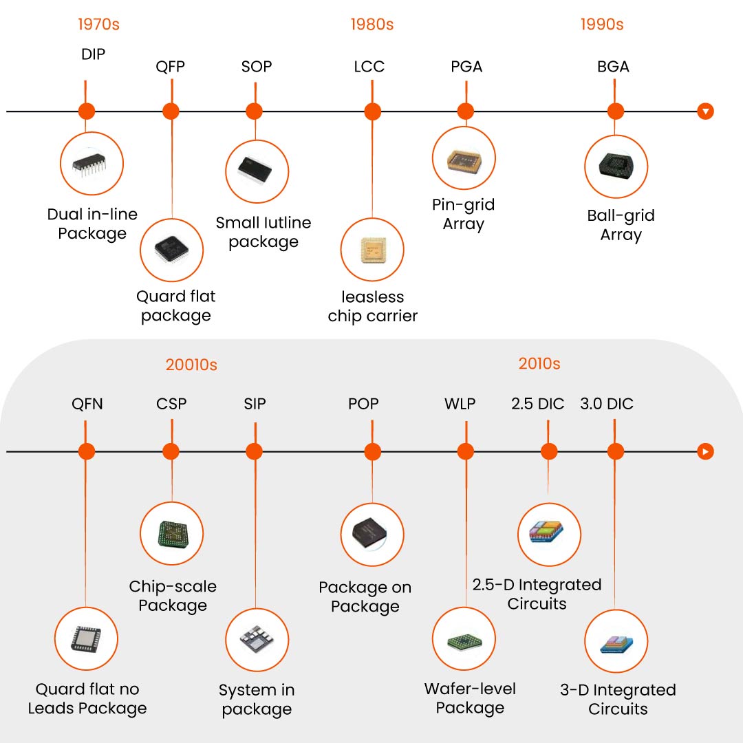
Source: AnySilicon
Wafer-level Packaging
In the conventional packaging process, the silicon wafer is initially divided into individual chips, which are subsequently attached to the printed circuit board (PCB) with electrical connections built. In contrast, wafer-level packaging operates differently by establishing electrical connections and molding at the wafer level before segmenting the chips using a laser. The primary distinction between wafer-level chip-scale packaging (WLCSP) and flip chips, concerning chip configuration, lies in the absence of a substrate between the die and the PCB in WLCSPs. Instead, redistribution layers (RDLs) take the place of the substrate, resulting in a more compact package and improved thermal conductivity.
Fig 2: Wafer Level Packaging
Source: AnySilicon, IEEE
Wafer-level packaging can be categorized into two primary types: fan-in and fan-out. In fan-in wafer-level packaging, typically employed for basic technology requirements in low-end mobile phones, the Redistribution Layers (RDLs) are directed toward the center of the die. Conversely, in fan-out packaging, introduced in 2007, the RDL and solder balls extend beyond the die's dimensions, allowing the chip to accommodate more inputs and outputs while maintaining a slim profile. Fan-out packaging manifests in three variations: core, high density, and ultrahigh density. Core packaging is primarily utilized in automotive and network applications that don't demand cutting-edge technology, such as radio frequency and infotainment chips. High and ultrahigh-density variants find extensive usage in mobile applications and are expected to expand into select network and high-performance computing applications. Taiwan Semiconductor Manufacturing Company (TSMC) holds the distinction of being the world's largest producer of Wafer-level Chip-Scale Packages (WLCSPs).
Wafer level packaging market is expected to grow at a rate of 21.0% for the forecast period of 2021 to 2028. Wafer level packaging market report analyses the growth, which is currently growing due to the impending need for circuit miniaturization in microelectronic devices.
To know more about the study, visit https://www.databridgemarketresearch.com/reports/global-wafer-level-packaging-market
Fig 3: Fan in and Fan Out Package Types
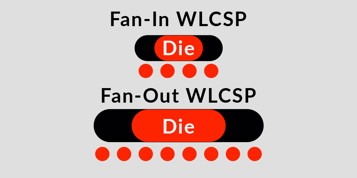
Source: AnySilicon, IEEE
Over the past decade, significant progress has been made in the realm of stacked Wafer-level Chip-Scale Packages (WLCSP). This advancement enables the incorporation of multiple integrated circuits within a single package, serving both heterogeneous bonding, which integrates logic and memory chips, and the stacking of memory chips.
In the case of 2.5-D stacking, two or more chips are positioned side by side with an interposer facilitating connections between the dies. Various categories of 2.5-D stacking exist, depending on the type of interposer employed:
In the domain of 3-D stacking, multiple chips are stacked atop each other, either with or without an interposer. There are two primary types of 3-D stacking:
Traditional Packaging Limitations
Advancements in Chip Packaging
To address these limitations and gain a competitive edge, semiconductor companies have been investing in advanced chip packaging technologies. Several key advancements have emerged in recent years:
Interposer + Substrate
The foundational piece that makes advanced packaging possible is interposers. These thin substrates provide a base where individual dies will be placed, as well as tiny interconnects to attach to the main packaging substrate. Interposers used in these advanced packages are made of three possible materials:
Fig 4: Interposer + Substrate
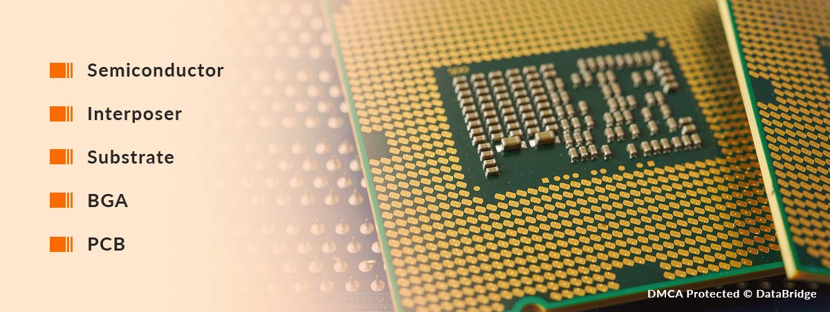
Source: SMG
2.5D and 3D Packaging
2.5D and 3D packaging technologies involve stacking multiple chips on top of each other or adjacent to each other, using through-silicon vias (TSVs) to enable communication between layers. These technologies provide several benefits:
Fig 5: Left: Flipchip packaging concept. Center: 2.5D integration on an interposer. Right: 3D integration on an interposer.
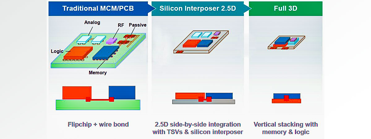
Source: eInfochips
Advanced Materials
New materials have been developed to enhance the performance and efficiency of chip packaging:
Heterogeneous Integration
Heterogeneous integration involves combining different types of chips, such as CPUs, GPUs, AI accelerators, and sensors, in a single package. This approach offers several advantages:
Package-on-Package (PoP)
The package-on-package (PoP) concept is similar to a set of stacked BGAs. Multiple packages are constructed with BGA footprint and stacked vertically on successive substrate layers. In theory, this allows an existing package to be integrated directly on top of another package, similar to stacking multiple PCBs on top of each other. The lowest-level ball array is soldered to a PCB and provides access to the remaining portions of the package.
Fig 6: Package-on-Package (PoP)
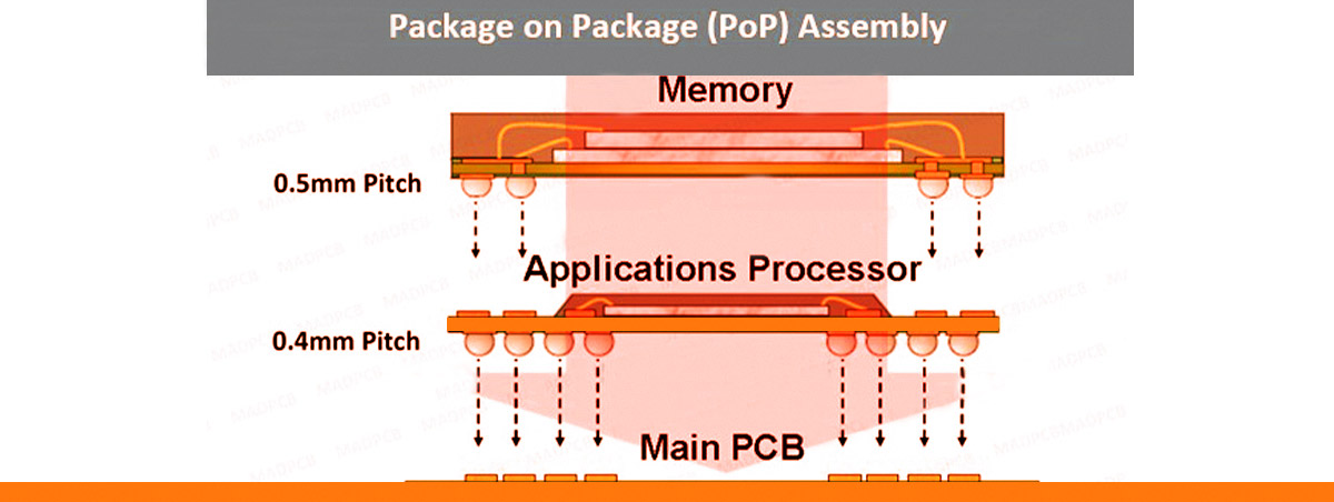
Source: MADPCB
This is less of a specific packaging structure and more of a design methodology or type of packaging design. All systems-in-package (SIPs) follow a specific design concept: the package attempts to integrate as many components as possible so that the package contains an entire system, often being designed for a specific application.
Any of the following elements can be present in SIPs for advanced components:
Some fresh components are being designed as SIPs or SoCs with advanced reconfigurable logic, meaning an FPGA coprocessor is implemented in the package. This gives the component designer significant flexibility to tailor a SIP to their end product, as well as create a warning for later reconfigurability once the product is deployed in the field.
Fig 7: System-in-Package (SIP)
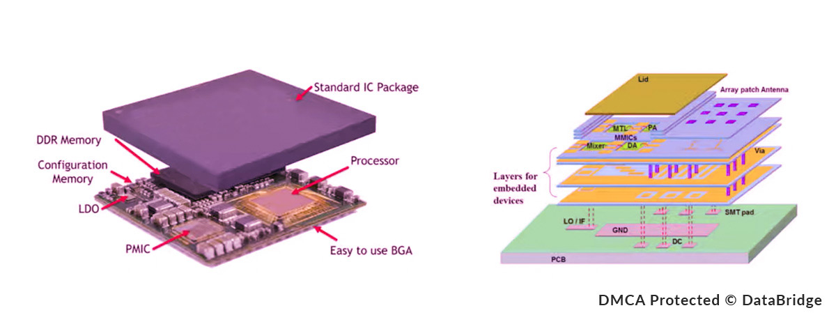
Source: AnySilicon
Finally, a distinction is made between a system-on-chip (SoC) and an SIP. An SoC is still an SIP, but it only exists as a single chip, which may not be designed as an interposer. For this reason, some SoC products are placed in traditional packaging or integrated packaging with an interposer and substrate. SIPs also provide the integration seen in SoCs, but they implement the type of integration with multiple components outlined above.
Data Bridge Market Research analyses that the system in package (SIP) market was valued at USD 23.51 billion in 2021 and is expected to reach USD 49.84 billion by 2029, registering a CAGR of 9.85% during the forecast period of 2022 to 2029. The market report curated by the Data Bridge Market Research team includes in-depth expert analysis, import/export analysis, pricing analysis, production consumption analysis, and pestle analysis.
https://www.databridgemarketresearch.com/reports/global-system-in-package-sip-market
Market Dynamics
Market expansion depends significantly on end customers, including automotive original equipment manufacturers (OEMs) and manufacturers of household appliances. An increasing number of end customers are actively seeking providers specializing in advanced packaging. This demand is driven by the growing necessity for fast and dependable computing, particularly in applications such as autonomous vehicles. For semiconductor manufacturers, especially logic integrated device manufacturers (IDMs) and foundries, advanced packaging stands as a crucial competitive advantage. To attract and retain high-value fabless semiconductor customers, manufacturers must be open to collaborative efforts in developing advanced packaging solutions. While fabless semiconductor companies maintain full control over the chip-planning process until large-scale production commences, there remains an opportunity for manufacturers to contribute value. Joint development efforts typically take place during the chip architecture design phase and initial shuttle runs for design validation. The need for such collaboration is projected to rise due to the escalating demand for higher-performance chips and the increasing complexity of chip designs resulting from advanced packaging techniques.
Fast followers may encounter significant challenges when attempting to catch up with market leaders. This is primarily because substantial technology investments are necessary to assure customers of the production volume required to support their products. Furthermore, although fast followers may possess research and development (R&D) level packaging technology for fan-out and 2.5-D packaging, they typically lack production experience, a crucial factor in achieving high production yield.
To address these challenges, packaging companies must proactively seek anchor customers during the early stages of development. Positioning their companies as willing partners in the manufacturing of advanced packaging solutions from the design phase becomes instrumental in acquiring customers.
Advanced packaging necessitates alterations in both end-user software and hardware architectures. Therefore, packaging design should be considered during the initial architectural planning stage. Support from backend providers during this phase can alleviate the burden of adopting advanced packaging. Once a customer selects an advanced packaging vendor, they are likely to continue their partnership with that vendor for future projects.
To enhance their design capabilities, companies have the option to collaborate with or invest in a design house. These design houses play a critical role throughout the entire chip-making process, encompassing intellectual property (IP) development, design, and production. Owing an IP pool can expedite customer design requirements, helping them avoid redundant designs and resource expenditures. Design houses should offer comprehensive front- and back-end services, including register-transfer-level design, high-level functional descriptions, logic testing, and place and route services.
Another potentially valuable proposition for chip manufacturers is to secure design capabilities and offer turnkey solutions, spanning from design to wafer manufacturing, packaging, and testing. This holistic offering provides customers with a convenient one-stop solution for their semiconductor needs.
Regarding manufacturing, there are two pivotal technological capabilities that manufacturers must master for 2.5-D and 3-D packaging. For 2.5-D packaging, proficiency is required in handling emerging interposer solutions that incorporate novel materials and manufacturing methodologies like silicon, redistribution layers (RDL), and glass. In the case of 3-D packaging, the latest technology, hybrid bonding, necessitates chemical mechanical planarization to ensure even flatness across various substances and prevent dishing. Additionally, high interconnect accuracy through disk-to-wafer capabilities in both equipment and expertise is crucial.
Competitive Edge Through Advanced Chip Packaging
The adoption of advanced chip packaging techniques provides companies with a significant competitive edge:
The major underlying trend in advanced packaging has been the integration or packing of more features and circuit blocks into smaller spaces, all operating at faster speeds. To facilitate this type of feature packaging, the industry has developed multiple types of semiconductor packaging designs that enable the continued integration of diverse features.
Here are a few instances of how companies are using ACP to offer more components to clients and gain a competitive edge:
By offering more components to clients through ACP, companies can gain a competitive edge in the marketplace.
The semiconductor packaging market is expected to witness market growth at a rate of approximately 8.00% in the forecast period of 2021 to 2028, and will reach a value of 53,676.97 by 2028. Data Bridge Market Research report on the semiconductor packaging market provides analysis and insights regarding the various factors expected to be prevalent throughout the forecast period while providing their impacts on the market’s growth. The rise in the packaging sector globally is escalating the growth of the semiconductor packaging market.
https://www.databridgemarketresearch.com/reports/global-semiconductor-packaging-market
Conclusion
In the fast-paced world of semiconductor technology, advancements in chip packaging are a critical factor in gaining a competitive edge. Through techniques such as 2.5D and 3D packaging, advanced materials, and heterogeneous integration, companies can offer more components and functionalities to their clients without compromising on performance, size, or power efficiency. These advancements not only drive innovation but also ensure that semiconductor companies remain at the forefront of delivering cutting-edge solutions to meet the demands of an increasingly connected world. Embracing these advancements in chip packaging will be essential for companies seeking to thrive in the ever-evolving landscape of electronic devices.
DBMR has served more than 40% of Fortune 500 firms internationally and has a network of more than 5000 clients. Our Team would be happy to help you with your queries. Visit, https://www.databridgemarketresearch.com/contact
Contact Us